

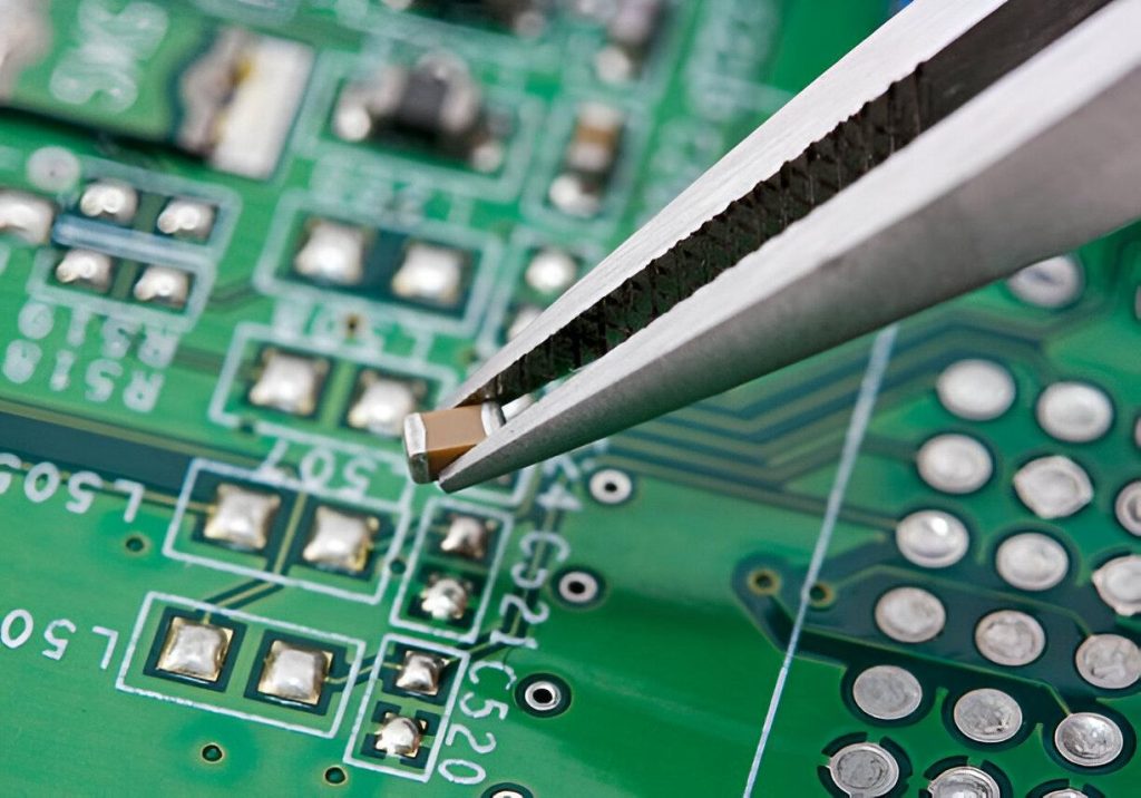
As electronic devices continue to become smaller, faster, and more powerful, printed circuit board (PCB) technology has evolved to accommodate increasing circuit complexity. Modern smartphones, medical devices, automotive electronics, aerospace systems, and telecommunications equipment all require compact PCB layouts capable of supporting thousands of electrical connections within limited board space. One of the key innovations that enables these advanced designs is the use of Blind and Buried Vias.
Unlike traditional through-hole vias that pass through the entire PCB, blind and buried vias provide more efficient routing by connecting only specific PCB layers. This advanced interconnection technology allows engineers to maximize routing density, improve signal integrity, and reduce board size without sacrificing performance. As a result, blind and buried vias have become a standard feature in high-density interconnect (HDI) PCBs and other advanced multilayer circuit boards.
However, manufacturing these sophisticated structures requires specialized equipment, precise process control, and extensive engineering expertise. Choosing an experienced Blind and Buried Vias PCB Manufacturer is essential to ensure reliable fabrication, accurate layer alignment, and long-term electrical performance.
This article explores what blind and buried vias are, how they are manufactured, their advantages, common applications, and why selecting the right PCB manufacturing partner is critical for high-performance electronics.
What Are Blind and Buried Vias?
Blind and Buried Vias are specialized plated holes used to create electrical connections between selected layers of a multilayer printed circuit board without passing through the entire board thickness.
A blind via connects an outer layer to one or more internal layers but does not extend completely through the PCB. Since it occupies only part of the board thickness, it frees additional routing space on other layers and allows designers to place more components in compact layouts.
A buried via, on the other hand, connects only internal copper layers and remains completely enclosed within the PCB structure. Because buried vias never reach the board surface, they provide internal electrical connections without occupying valuable space on the outer layers.
Together, blind and buried vias allow engineers to design highly compact circuit boards while maintaining reliable electrical interconnections throughout complex multilayer structures.
Why Blind and Buried Vias Are Important
The growing demand for compact electronics has made Blind and Buried Vias increasingly important in PCB design. Traditional through-hole vias consume routing space on every PCB layer, limiting design flexibility as circuit density increases.
Blind and buried vias eliminate many of these limitations by connecting only the layers that require electrical continuity. This approach leaves additional routing channels available for high-speed signals, power distribution, and component placement.
The reduced number of through-hole structures also improves signal integrity by minimizing unwanted electrical effects such as signal reflections, parasitic capacitance, and inductance. These improvements are especially valuable in high-frequency communication systems, high-speed digital circuits, and advanced computing platforms.
As PCB designs continue to evolve toward greater functionality within smaller dimensions, blind and buried vias provide the routing efficiency needed to support increasingly sophisticated electronic products.
The Manufacturing Process for Blind and Buried Vias
Producing Blind and Buried Vias requires a more advanced manufacturing process than conventional through-hole PCB fabrication. The process begins with detailed engineering analysis to determine which layers require blind or buried interconnections based on the PCB stackup and routing requirements.
Buried vias are typically fabricated during the early stages of multilayer PCB construction. Individual internal layers are drilled, plated, inspected, and laminated together before the remaining outer layers are added to the board.
Blind vias are commonly produced using precision laser drilling or controlled-depth mechanical drilling after partial lamination. Once the via holes have been created, copper plating establishes reliable electrical connections between the required PCB layers.
Throughout fabrication, strict control of drilling accuracy, copper plating thickness, layer registration, and lamination quality is essential to ensure reliable via performance.
Following manufacturing, extensive inspection and electrical testing verify that every blind and buried via functions correctly before the completed PCB proceeds to assembly.
Advantages of Blind and Buried Vias
One of the most significant benefits of Blind and Buried Vias is increased routing density. By reducing the number of through-hole connections, designers gain additional routing space that supports more complex circuits within smaller PCB dimensions.
These advanced vias also improve electrical performance by shortening signal paths and reducing parasitic electrical effects. This contributes to better signal integrity, particularly in high-speed digital systems and RF applications.
Another important advantage is enhanced component placement flexibility. Since fewer vias occupy surface routing areas, engineers can position components closer together, enabling higher packaging density for compact electronic products.
Blind and buried vias also contribute to improved thermal management by allowing more efficient power plane design and optimized copper distribution throughout multilayer boards.
Although manufacturing costs are generally higher than traditional PCB fabrication, the performance improvements often justify the investment for advanced electronic applications.
Applications of Blind and Buried Vias
Blind and Buried Vias are widely used in products that require high-density circuit layouts and superior electrical performance. Consumer electronics manufacturers utilize this technology in smartphones, tablets, laptops, wearable devices, gaming systems, and smart home products where compact designs are essential.
Automotive electronics also rely on advanced via structures for electric vehicle control units, battery management systems, advanced driver assistance systems, infotainment platforms, radar modules, and safety electronics operating in demanding environments.
Medical device manufacturers use blind and buried vias in portable diagnostic equipment, patient monitoring systems, imaging devices, laboratory analyzers, and implantable medical electronics that require compact yet highly reliable PCB designs.
Telecommunications equipment, networking hardware, aerospace electronics, defense systems, industrial automation equipment, renewable energy systems, robotics, and Internet of Things devices also benefit from the routing efficiency and signal performance provided by blind and buried vias.
These applications demonstrate how advanced via technology supports the continuing miniaturization of modern electronic products.
Choosing a Blind and Buried Vias PCB Manufacturer
Selecting an experienced Blind and Buried Vias PCB Manufacturer is essential because these PCB structures require specialized fabrication capabilities that exceed conventional PCB manufacturing.
Professional manufacturers provide engineering support during the design stage, helping customers optimize layer stackups, via placement, routing strategies, and manufacturability before production begins.
Modern fabrication facilities utilize laser drilling systems, high-precision mechanical drilling equipment, advanced lamination presses, automated copper plating lines, laser direct imaging, and computerized process control to achieve the accuracy required for complex via structures.
Many manufacturers also offer integrated services including PCB fabrication, HDI manufacturing, prototype development, PCB assembly, component sourcing, electrical testing, and supply chain management. This comprehensive approach simplifies project management while improving manufacturing consistency.
Working with a manufacturer experienced in advanced multilayer PCB technology helps reduce production risks and ensures dependable long-term performance.
Quality Assurance in Blind and Buried Via Manufacturing
Quality assurance plays a critical role in the production of Blind and Buried Vias because internal interconnections cannot be easily inspected after PCB assembly. Manufacturers begin by reviewing customer design files to verify via dimensions, stackup configuration, drilling requirements, and plating specifications.
During fabrication, automated systems continuously monitor drilling accuracy, layer alignment, copper plating thickness, lamination quality, and registration between individual PCB layers.
Following manufacturing, Automated Optical Inspection, X-ray inspection, electrical continuity testing, impedance verification, and cross-sectional analysis confirm that blind and buried vias meet design requirements.
Reliability testing may also include thermal cycling, vibration testing, solderability evaluation, environmental stress screening, and mechanical durability testing to ensure long-term via integrity under demanding operating conditions.
Leading manufacturers maintain internationally recognized certifications such as ISO 9001, IPC standards, UL certification, IATF 16949 for automotive electronics, ISO 13485 for medical devices, AS9100 for aerospace manufacturing, and RoHS compliance. These quality systems demonstrate a commitment to producing highly reliable multilayer PCBs for critical electronic applications.
Conclusion
Blind and Buried Vias have become indispensable technologies for modern PCB design, enabling engineers to create smaller, more complex, and higher-performing electronic products. By improving routing density, enhancing signal integrity, supporting compact component placement, and optimizing multilayer PCB layouts, these advanced interconnection structures help meet the growing demands of today’s electronics industry.
An experienced Blind and Buried Vias PCB Manufacturer combines advanced fabrication technology, engineering expertise, and rigorous quality assurance to produce reliable multilayer circuit boards for industries including consumer electronics, automotive, medical devices, telecommunications, industrial automation, aerospace, and defense. By partnering with a manufacturer specializing in advanced PCB technologies, businesses can successfully develop high-density electronic products that deliver exceptional performance, reliability, and long-term durability.
